circuits
schematics
diagrams
FreeCircuits.net


16-bit ADC provides 19-bit resolution
By internum
Many data-acquisition systems require both high accuracy and a fast acquisition rate. These attributes allow the system to detect small data signals and to group more sensor channels into the same system. With more channels, the system can be smaller, less expensive, and less power-consuming. Long-distance optical communications and medical equipment, such as CT scanners, can benefit from a fast and accurate data-acquisition system. Optical power systems, such as laser pumps, need to constantly monitor their power levels. In such systems, the incoming laser-power range and the laser control-loop response time are such that the system needs a dynamic range of 90 dB or more and a sampling rate of 1M sample/sec. In CT scanners, 16- to 22-bit resolution is necessary for the data-acquisition system to process the large dynamic range of the X-rays through various body tissues. A large number of photodetectors (more data-acquisition channels) and high data accuracy improve the image resolution.


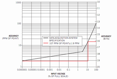
Figure 1. Using a programmable-gain amplifier ahead of an ADC increases the accuracy of a 16-bit ADC to 19 bits.
These two examples show the need for relative accuracy, as opposed to absolute accuracy. Although it's important to be able to detect a 10-nW change in an optical power of 1 µW, it is almost irrelevant to see the same 10-nW difference between 1 mW and 1.00001 mW. However the ADC's accuracy appears under the integral-nonlinearity specification as an absolute error. For the best relative accuracy, a classic solution is to use a programmable-gain amplifier in front of an accurate ADC. The AD7677 ADC specifies ±15-ppm of full-scale nonlinearity (±1 LSB at the 16-bit level). A programmable-gain amplifier ahead of this converter must be able to settle quickly enough with the same resolution and speed as the ADC. It also must have the lowest noise possible, because the amplifier sets the SNR of the data-acquisition system. To meet these challenges, the amplifier in this design uses an AD8021, an op amp combing speed, accuracy, and fast settling time. The noise density of the AD8021 is only 2 nV/ . Figure 1 shows how the gain settings of the programmable-gain amplifier divide the specified accuracy of the ADC. The system reaches 19-bit accuracy when the input level is low.
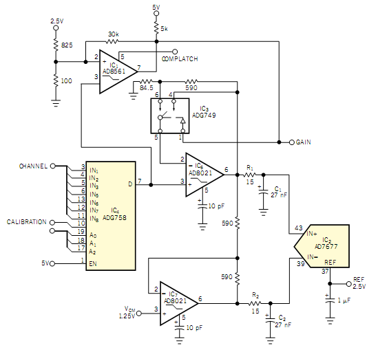
Figure 2. This system provides 19-bit accuracy by combining a programmable-gain amplifier with a 16-bit ADC.
Relative accuracy is normally specified as parts per million of reading plus or minus the absolute minimum error. The circuit in Figure 2 can achieve a relative accuracy of 107 ppm±1.9-ppm maximum error. Analog multiplexer IC4 combines many lower bandwidth channels to take advantage of the 1M-sample/sec sampling rate of the ADC. Because the programmable-gain amplifier presents a high input impedance to the multiplexer, you can cascade the multiplexer, thus increasing the number of channels. The multiplexer also provides a simple way to calibrate the offset and gain errors at each gain setting by applying a calibration-reference voltage to one of the multiplexer's input ports. You need to calibrate only at power-up or when operating conditions, such as temperature, change. The amplification chain comprises the multiplexer, the comparator, and the amplifier on one side and the ADC on the other side. The successive-approximation structure of the AD7677 ADC allows the individual sections in the amplification chain to work simultaneously. While the ADC converts one sample, the comparator/amplifier can settle the following channel. Therefore, the data-acquisition system can operate at the ADC's maximum sampling rate.
Shortly after the analog multiplexer settles, the fast comparator, IC1, applies the appropriate gain setting. The comparator's thresholds are such that the amplifier does not saturate or clip the signal after amplification by IC6 and IC7. The AD8561 comparator has a response time of 7 nsec. It integrates a latch signal that holds the gain constant during the time the amplifier settles and the ADC acquires the signal. The usual programmable-gain-amplifier configuration requires the user to predict the amplifier's gain setting before applying the signal at the input. The programmable-gain amplifier in Figure 2 has an "autorange" feature that selects the most appropriate programmable-gain amplifier gain to maximize accuracy without incurring saturation or clipping. The comparator incorporates hysteresis to reduce gain-setting change when signals are close to the limits of an individual gain range. The circuit automatically boosts the ADC accuracy to 19 bits while maintaining a full-speed sampling rate of 1M sample/sec.
IC6 amplifies the multiplexer signal using one of two possible gain settings: 1 or 8. You can modify the feedback network to provide different gains to a maximum of 25. The analog switch, IC3, controls the gain setting. The high gain-bandwidth product of the AD8021 op amp provides more than enough bandwidth, so its compensation capacitor remains the same for all gains. Amplifier IC7 generates the differential signal for the ADC. The settling times of the comparator and the amplifier and the acquisition time of the ADC are all significantly less than the ADC's full conversion period of 1 µsec. The RC noise filters at the two ADC inputs, R1/C1 and R2/C2, use this extra time. These filters limit the noise bandwidth of the programmable-gain amplifier, which is the main noise source of the data-acquisition system when IC7 operates at a gain of –1.
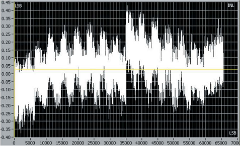
Figure 3. This plot shows the differential nonlinearity of a data-acquisition system for all possible ADC codes.
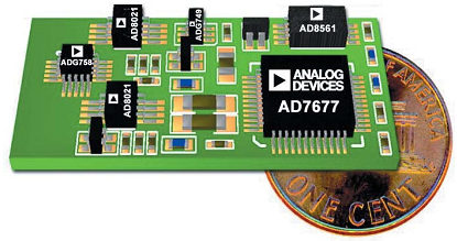
Figure 4. The dime shows the relative size of the complete data-acquisition system.
Figure 3 shows the circuit's nonlinearity. The photo shows a maximum nonlinearity of 0.44 LSB and a minimum of –0.37 LSB for the highest gain setting, which poses the most difficult challenge. This nonlinearity corresponds to a typical error of ±0.9 ppm. At a gain of 8, output noise is 85 µV rms. If desired, you can further reduce the noise by using software averaging. Figure 4 shows the complete data-acquisition system assembled using the AD7677 evaluation board. The pc-board area measures 15×30 mm.
 1751
1751  19 September 2009