circuits
schematics
diagrams
FreeCircuits.net


The A/D Easily Allows Many Unusual Applications
By internum
Accommodation of Arbitrary Analog Inputs Two design features of the ADC0801 series of A/D converters provide for easy solutions to many system design problems. The combination of differential analog voltage inputs and a voltage reference input which can range from near zero to 5VDC are key to these application advantages.
In many systems the analog signal which has to be converted does not range clear to ground (0.00 VDC) nor does it reach up to the full supply or reference voltage value. This presents two problems: 1) a “zero-offset” provision is needed—and this may be volts, instead of the few millivolts which are usually provided; and 2) the “full scale” needs to be adjusted to accommodate this reduced span. (“Span” is the actual range of the analog input signal, from VIN MIN to VIN MAX.) This is easily handled with the converter as shown in Figure 1.

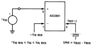
Figure 1. Providing Arbitrary Zero and Span Accommodation
Note that when the input signal, VIN, equals VIN MIN the “differential input” to the A/D is zero volts and therefore a digital output code of zero is obtained. When VINequals VIN MAX, the “differential input” to the A/D is equal to the “span” (for reference applications convenience, there is an internal gain of two to the voltage which is applied to pin 9, the VREF/2 input), therefore the A/D will provide a digital full scale. In this way a wide range of analog input voltages can be easily accommodated.
An example of the usefulness of this feature is when operating with ratiometric transducers which do not output the complete supply voltage range. Some, for example, may output 15% of the supply voltage for a zero reading and 85% of the supply for a full scale reading. For this case, 15% of the supply should be applied to the VIN(−) pin and the VREF/2 pin should be biased at one-half of the span, which is 1⁄2 (85%–15%) or 35% of the supply. This properly shifts the zero and adjusts the full scale for this application. The VIN(−) input can be provided by a resistive divider which is driven by the power supply voltage and the VREF/2 pin should be driven by an op amp. This op amp can be a unity-gain voltage follower which also obtains an input voltage from a resistive divider. These can be combined as shown in Figure 2.
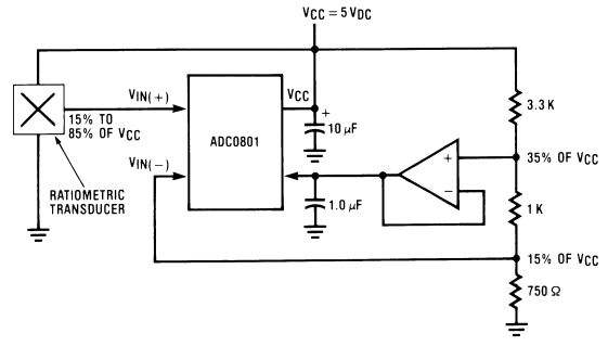
Figure 2. Operating with a Ratiometric Transducer which Outputs 15% to 85% of VCC
This application can allow obtaining the resolution of a greater than 8-bit A/D. For example, 9-bit performance with the 8-bit converter is possible if the span of the analog input voltage should only use one-half of the available 0V to 5V span. This would be a span of approximately 2.5V which could start anywhere over the range of 0V to 2.5VDC.
The RC network on the output of the op amp of Figure 2 is used to isolate the transient displacement current demands of the VREF/2 input from the op amp.
A question arises as to how small in value the span can be made. An ADC0801 part is shown in Figure 3 where the VREF/2 voltage is reduced in steps: from A), 2.5V (for a full scale reading of 5V); to B), 0.625V (for a full scale reading of 1.25V—this corresponds to the resolution of a 10-bit converter over this restricted range); to C), 0.15625V (for a full scale reading of 0.3125V—which corresponds to the resolution of a 12-bit converter). Note that at 12 bits the linearity error has increased to 1⁄2 LSB.
For these reduced reference applications the offset voltage of the A/D has to be adjusted as the voltage value of the LSB changes from 20 mV to 5 mV and finally to 1.25 mV as we go from A) to B) to C). This offset adjustment is easily combined with the setting of the VIN MIN value at the VIN(−) pin.
Operation with reduced VREF/2 voltages increases the requirement for good initial tolerance of the reference voltage (or requires an adjustment) and also the allowed changes in the VREF/2 voltage over temperature are reduced.
An interesting application of this reduced reference feature is to directly digitize the forward voltage drop of a silicon diode as a simple digital temperature sensor.
 825
825  19 September 2009