circuits
schematics
diagrams
FreeCircuits.net


12-Bit Sampling A/D Converter Conserves Power
By internum
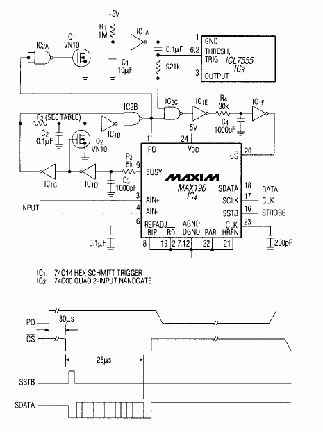
The 5Vm 12-bit, A/D-converter circuit of Figure 1 draws minimal supply current at low conversion rates. Typical power consumption is ¼mW at 1 sample/sec, ½mW at 90 samples/sec, and 4.3mW at 1.5k samples/sec. The converter circuit is complete with track/hold, clock, voltage reference, serial data output, and all necessary peripheral logic.
12-Bit Sampling A/D Converter Conserves Power circuit
Figure 1. This 12-bit sampling A/D converter circuit draws as little as 50µA from a 5V supply. The timer (IC3) assures proper startup when power is applied.
The overall circuit requires no external control because the A/D converter operates in a self-start mode driven by its internal; clock. Peripheral logic generates the control signals necessary to power up the converter, wait 30µsec, start a conversion, power down for a fixed interval following the end of conversion, and repeat.
CMOS logic assures minimal current drain. The circuit employs a discrete one-shot (IC1B and IC2B) to avoid the higher quiescent current associated with an integrated version. R2 affects the sample rate and overall power dissipation:
Table 1.
| R2 Value (Ω) |
Sample Rate | Supply Current | |
| Complete Circuit (µA) |
A/D converter (µA) |
||
| 1M | 1Hz (approx.) | 50 | 25 |
| 91k | 90Hz | 100 | 40 |
| 15k | 524Hz | 335 | 121 |
| 9.1K | 840Hz | 510 | 180 |
| 4.7k | 1500Hz | 860 | 297 |
During normal operation, conversions are initiated by active-low BUSY signals that propagate around the main loop (via IC2B andIC2c) and cause high-to-low transitions at CS. But, during power-up the logic may assume an illegal state that causes IC2B output to remain High. Under that condition the upper loop becomes active: Q1 remains off, C1 charges towards 5V, and the IC1A output goes low, providing a ground for the CMOS timer IC3.
Timer signals the toggle IC2C, Providing a needed transition at the active-low CS input. Normal operation resumes because the resulting lows at PD cause C1 to discharge repeatedly, disabling the upper loop. This arrangement assures startup while maintaining a low quiescent current in the startup circuit.
The application as shown provides the digital output in serial form, though the converter (IC4) offers 8-bit parallel data as well. As each conversion begins, twelve bits of serial data shift out at the SDATA terminal in sync with the internally generated SCLK. (Because SCLK disappears after bit twelve, SDATA and SCLK can connect directly to a shift register.) An additional output SSTB (a framing signal that goes high during the MSB decision) provides an interface for the TMS320 family µPs.
The circuit includes four RC networks in addition to that of the timer: R1C1 sets the inactive period at PD, before the upper-loop startup circuit takes over. R2C2 sets the power-down interval between conversions. R3C3 sets a delay between the end of conversion and the converter's power-saving shutdown. R4C4 sets a delay between powerup and the start of a conversion.
 720
720  19 September 2009