circuits
schematics
diagrams
FreeCircuits.net


The Full-Wave Rectifier and Averaging Filter
By internum
The circuit shown in Figure 1 is the heart of an average reading, rms calibrated AC voltmeter. As shown, it is a rectifier and averaging filter. Deletion of C2 removes the averaging function and provides a precision full-wave rectifier, and deletion of C1 provides an absolute value generator.
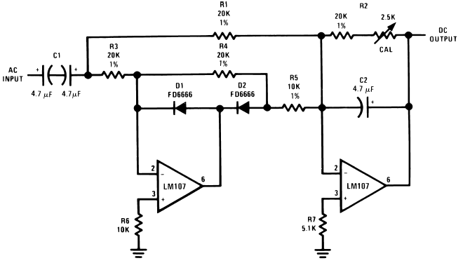
Figure 1. Full-Wave Rectifier and Averaging Filter
Circuit operation may be understood by following the signal path for negative and then for positive inputs. For negative signals, the output of amplifier A1 is clamped to +0.7V by D1 and disconnected from the summing point of A2 by D2. A2 then functions as a simple unity-gain inverter with input resistor, R1, and feedback resistor, R2, giving a positive going output.
For positive inputs, A1 operates as a normal amplifier connected to the A2 summing point through resistor, R5. Amplifier A1 then acts as a simple unity-gain inverter with input resistor, R3, and feedback resistor, R5. A1 gain accuracy is not affected by D2 since it is inside the feedback loop. Positive current enters the A2 summing point through resistor, R1, and negative current is drawn from the A2 summing point through resistor, R5. Since the voltages across R1 and R5 are equal and opposite, and R5 is one-half the value of R1, the net input current at the A2 summing point is equal to and opposite from the current through R1 and amplifier A2 operates as a summing inverter with unity gain, again giving a positive output.
The circuit becomes an averaging filter when C2 is connected across R2. Operation of A2 then is similar to the Simple Low Pass Filter previously described. The time constant R2C2 should be chosen to be much larger than the maximum period of the input voltage which is to be averaged.
Capacitor C1 may be deleted if the circuit is to be used as an absolute value generator. When this is done, the circuit output will be the positive absolute value of the input voltage.
The amplifiers chosen must be compensated for unity-gain operation and R6 and R7 must be chosen to minimize output errors due to input offset current.
 4842
4842  10 December 2007