circuits
schematics
diagrams
FreeCircuits.net

The Reset Stabilized Amplifier
By internum
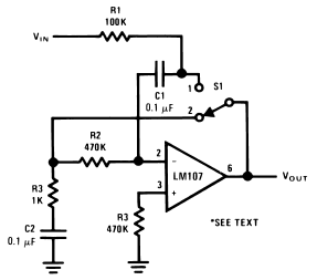
The reset stabilized amplifier is a form of chopper-stabilized amplifier and is shown in Figure 1. As shown, the amplifier is operated closed-loop with a gain of one.

Figure 1. Reset Stabilized Amplifier
The connection is useful in eliminating errors due to offset voltage and bias current. The output of this circuit is a pulse whose amplitude is equal to VIN. Operation may be understood by considering the two conditions corresponding to the position of S1. When S 1 is in position 2, the amplifier is connected in the unity gain connection and the voltage at the output will be equal to the sum of the input offset voltage and the drop across R2 due to input bias current. The voltage at the inverting input will be equal to input offset voltage. Capacitor C1 will charge to the sum of input offset voltage and VIN through R1. When C1 is charged, no current flows through the source resistance and R1 so there is no error due to input resistance. S1 is then changed to position 1. The voltage stored on C1 is inserted between the output and inverting input of the amplifier and the output of the amplifier changes by VIN to maintain the amplifier input at the input offset voltage. The output then changes from (VOS + IbiasR2) to (VIN + IbiasR2) as S1 is changed from position 2 to position 1. Amplifier bias current is supplied through R2 from the output of the amplifier or from C2 when S1 is in position 2 and position 1 respectively. R3 serves to reduce the offset at the amplifier output if the amplifier must have maximum linear range or if it is desired to DC couple the amplifier.
An additional advantage of this connection is that input resistance approaches infinity as the capacitor C1 approaches full charge, eliminating errors due to loading of the source resistance. The time spent in position 2 should be long with respect to the charging time of C1 for maximum accuracy.
The amplifier used must be compensated for unity gain operation and it may be necessary to overcompensate because of the phase shift across R2 due to C1 and the amplifier input capacity. Since this connection is usually used at very low switching speeds, slew rate is not normally a practical consideration and overcompensation does not reduce accuracy.
 1454
1454 ![]() 10 December 2007
10 December 2007
