circuits
schematics
diagrams
FreeCircuits.net


The Inverting Amplifier
By internum
The basic operational amplifier circuit is shown in Figure 1. This circuit gives closed-loop gain of R2/R1 when this ratio is small compared with the amplifier open-loop gain and, as the name implies, is an inverting circuit. The input impedance is equal to R1. The closed-loop bandwidth is equal to the unity-gain frequency divided by one plus the closed-loop gain.
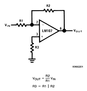
Figure 1. Inverting Amplifier
For minimum error due to input bias current
The only cautions to be observed are that R3 should be chosen to be equal to the parallel combination of R1 and R2 to minimize the offset voltage error due to bias current and that there will be an offset voltage at the amplifier output equal to closed-loop gain times the offset voltage at the amplifier input.
Offset voltage at the input of an operational amplifier is comprised of two components, these components are identified in specifying the amplifier as input offset voltage and input bias current. The input offset voltage is fixed for a particular amplifier, however the contribution due to input bias current is dependent on the circuit configuration used. For minimum offset voltage at the amplifier input without circuit adjustment the source resistance for both inputs should be equal. In this case the maximum offset voltage would be the algebraic sum of amplifier offset voltage and the voltage drop across the source resistance due to offset current. Amplifier offset voltage is the predominant error term for low source resistances and offset current causes the main error for high source resistances.
In high source resistance applications, offset voltage at the amplifier output may be adjusted by adjusting the value of R3 and using the variation in voltage drop across it as an input offset voltage trim.
Offset voltage at the amplifier output is not as important in AC coupled applications. Here the only consideration is that any offset voltage at the output reduces the peak to peak linear output swing of the amplifier.
The gain-frequency characteristic of the amplifier and its feedback network must be such that oscillation does not occur. To meet this condition, the phase shift through amplifier and feedback network must never exceed 180В° for any frequency where the gain of the amplifier and its feedback network is greater than unity. In practical applications, the phase shift should not approach 180В° since this is the situation of conditional stability. Obviously the most critical case occurs when the attenuation of the feedback network is zero.
Amplifiers which are not internally compensated may be used to achieve increased performance in circuits where feedback network attenuation is high. As an example, the LM101 may be operated at unity gain in the inverting amplifier circuit with a 15 pF compensating capacitor, since the feedback network has an attenuation of 6 dB, while it requires 30 pF in the non-inverting unity gain connection where the feedback network has zero attenuation. Since amplifier slew rate is dependent on compensation, the LM101 slew rate in the inverting unity gain connection will be twice that for the non-inverting connection and the inverting gain of ten connection will yield eleven times the slew rate of the non-inverting unity gain connection. The compensation trade-off for a particular connection is stability versus bandwidth, larger values of compensation capacitor yield greater stability and lower bandwidth and vice versa.
The preceding discussion of offset voltage, bias current and stability is applicable to most amplifier applications and will be referenced in later sections.
 2269
2269  09 December 2007