circuits
schematics
diagrams
FreeCircuits.net

Differentiator
By internum

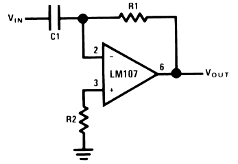
Figure 1. Differentiator

R1 = R2
For minimum offset error due to input bias current
The differentiator is shown in Figure 1 and, as the name implies, is used to perform the mathematical operation of differentiation. The form shown is not the practical form, it is a true differentiator and is extremely susceptible to high frequency noise since AC gain increases at the rate of 6 dB per octave. In addition, the feedback network of the differentiator, R1C1, is an RC low pass filter which contributes 90В° phase shift to the loop and may cause stability problems even with an amplifier which is compensated for unity gain.

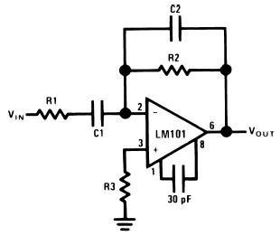
Figure 2. Practical Differentiator

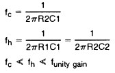
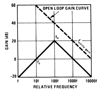
A practical differentiator is shown in Figure 2. Here both the stability and noise problems are corrected by addition of two additional components, R1 and C2. R2 and C2 form a 6 dB per octave high frequency roll-off in the feedback network and R1C1 form a 6 dB per octave roll-off network in the input network for a total high frequency roll-off of 12 dB per octave to reduce the effect of high frequency input and amplifier noise. In addition R1C1 and R2C2 form lead networks in the feedback loop which, if placed below the amplifier unity gain frequency, provide 90В° phase lead to compensate the 90В° phase lag of R2C1 and prevent loop instability. A gain frequency plot is shown in Figure 3 for clarity.

Figure 3. Differentiator Frequency Response
 2344
2344 ![]() 09 December 2007
09 December 2007
