circuits
schematics
diagrams
FreeCircuits.net


The Analog Multiplier
By internum
A simple embodiment of the analog multiplier is shown in Figure 1. This circuit circumvents many of the problems associated with the log-antilog circuit and provides three quadrant analog multiplication which is relatively temperature insensitive and which is not subject to the bias current errors which plague most multipliers.
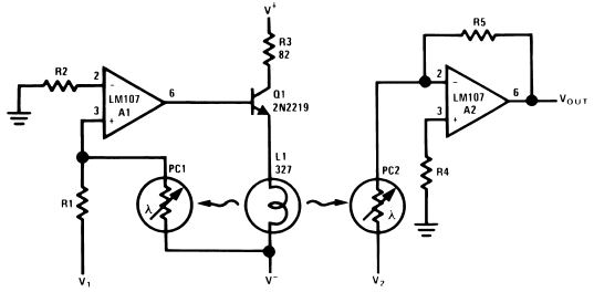
Figure 1. Analog Multiplier

Circuit operation may be understood by considering A2 as a controlled gain amplifier, amplifying V2, whose gain is dependent on the ratio of the resistance of PC2 to R5 and by considering A1 as a control amplifier which establishes the resistance of PC2 as a function of V 1. In this way it is seen that VOUT is a function of both V1 and V2.
A1, the control amplifier, provides drive for the lamp, L1. When an input voltage, V1, is present, L1 is driven by A1 until the current to the summing junction from the negative supply through PC1 is equal to the current to the summing junction from V1 through R1. Since the negative supply voltage is fixed, this forces the resistance of PC1 to a value proportional to R1 and to the ratio of V1 to V −. L1 also illuminates PC2 and, if the photoconductors are matched, causes PC2 to have a resistance equal to PC1.
A2, the controlled gain amplifier, acts as an inverting amplifier whose gain is equal to the ratio of the resistance of PC2 to R5. If R5 is chosen equal to the product of R1 and V−, then V OUT becomes simply the product of V1 and V2. R5 may be scaled in powers of ten to provide any required output scale factor.
PC1 and PC2 should be matched for best tracking over temperature since the T.C. of resistance is related to resistance match for cells of the same geometry. Small mismatches may be compensated by varying the value of R5 as a scale factor adjustment. The photoconductive cells should receive equal illumination from L1, a convenient method is to mount the cells in holes in an aluminum block and to mount the lamp midway between them. This mounting method provides controlled spacing and also provides a thermal bridge between the two cells to reduce differences in cell temperature. This technique may be extended to the use of FET’s or other devices to meet special resistance or environment requirements.
The circuit as shown gives an inverting output whose magnitude is equal to one-tenth the product of the two analog inputs. Input V 1 is restricted to positive values, but V2 may assume both positive and negative values. This circuit is restricted to low frequency operation by the lamp time constant.
R2 and R4 are chosen to minimize errors due to input offset current as outlined in the section describing the photocell amplifier. R3 is included to reduce in-rush current when first turning on the lamp, L1.
 2671
2671  10 December 2007